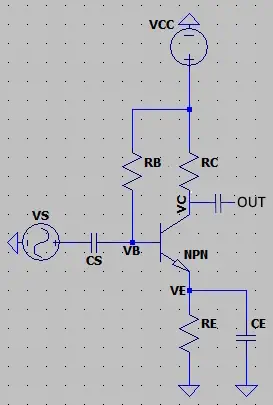
Before proceed reading see circuit diagram at end of page!
On collector we have a current "IC" causing a voltage drop "IC*RC" where "IC" is "IB" multipled by "hFE", on base we have a current "I RB" causing voltage drop to "VB" that need to be "VS" + "VE" + 0.6, on emitter we have a current "IB" plus "IC" causing a voltage drop on "RE" that need to be "VE"; for more gain we have "CE" 1/10th of "RE".
This is a calculator to compute the NPN Transistor in common emitter arrangement, Click on (i) for brief description of fields, it's possible to compute de CE (capacitor on emitter leg) on Capacitive Reactance Calculator using as frequency the minimum required to pass, and X(C) the value on the CE field.
| VCC (i) | |
| VC (i) | |
| VE (i) | |
| VS (i) | |
| Hfe (i) | |
| IC (i) | |
| VCE | |
| VB | |
| IB | |
| IE | |
| RC | |
| RE | |
| RB | |
| CE | |
| ZIN | |
| AV | |
| ZOUT | |
References:
Eletronics Tutorials NPN Common Emitter Eletronics Tutorials Transistor Impedance EletronicsHub Different configurations transistors ---| INDEX |---